Over the past couple of months there has been development work underway to implement support for custom pads shapes, and this new enhancement is now approaching the stage of being ready to deploy to the Beta group.
Before this happens though, I would like to share the current state of development with you and gather any final thoughts, ideas and suggestions as feedback.
In my initial blog on custom pad shapes I detailed the three options available to tackle this issue: either original primitives could be enhanced and used to define the custom shape of a pad (along with net propagation through copper and mask generation); the pad object could itself be enhanced with new capabilities; or finally, a new ‘custom shaped pad’ object could be added.
The feedback you provided in response to the blog was seminal in helping me understand your perspective and design this new feature.
The result is that three new enhancements have been added to support the generation and management of custom pads in Altium Designer:
1. General primitives can generate solder and paste mask expansions.
Any track, arc, fill or region on the top or bottom layer are now able to generate solder and paste masks. In a similar way to how the masks are generated for pads, the masks for these objects can be manually specified per object or globally with a design rule.
This eliminates the need for the current workaround used to generate paste mask and openings in the solder mask to match custom pad copper shape.
2. The nets on all copper primitives in a footprint are updated when synchronizing a PCB from the Project Schematics.
This removes the need to run “Update Free Primitives from Component Pads” after synchronizing the PCB with the project schematics
3. The “Create Region from Selected Objects” can now be launched from the PCB Library editor.
Regions are typically used as a workaround solution for the custom pad shapes. The addition of the “Create Region from Selected Objects” command to the PCB Library editor will make it easier to create the custom pads.
An added benefit of adding these enhancements to improve custom pad support is that they will prove useful in many other situations.
For example, when a Shielded Enclosure is used in a design, paste mask and solder mask openings are needed to match the copper shape on the PCB. In such a case the tracks and arcs that utilize the new Solder Mask and Paste Mask expansion properties can now accomplish the same task.
So with these three relatively simple enhancements, it is now much simpler to deal with custom pads.
Let me now show you what it takes to create custom shaped pads, link it to a component, and finally place and use it in a design. By way of example, I will use the SRR5028 series of inductors from Bourns.
In order to draw the footprint, I will start by creating regions on the top layer in the desired shape. Then a small pad will be placed in the centre of the regions and lastly the desired expansions masks will be set for each of the region.
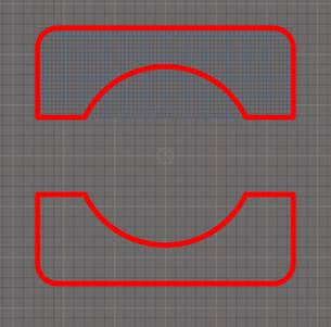
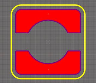
1. Following the suggested footprint in the datasheet I place an outline using tracks and arcs on the top layer in the PCB Library Editor. The customizable grids are helpful for precisely positioning the outline elements.

2. I create a region from the outline with the menu command Tools > Convert > Create region from selected primitives. Personally, from here I like to move the outline primitives to Mechanical Layer 31, which I consider a construction layer.

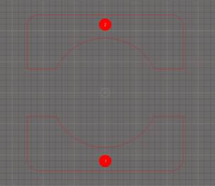
3. Then I place 0.5mm pads at the center of the regions. The region drawing mode has been set to draft in the below screenshot so that the pads are easier to see.

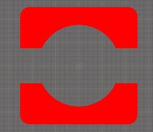
4. Next for each of the region that define a pad, I set the Solder Mask Expansion Mode and Paste Mask Expansion Mode to “From Rule”. Once placed on a PcbDoc the solder and mask expansions will be set as determined by the design rules.


5. Finally I add a silkscreen outline.

Now that the footprint for our inductor is drawn, we can continue by creating a schematic symbol that can be used in a design.
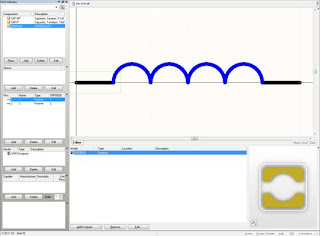
6. In the Schematic Library Editor I create a new component and assign it with the symbol reference of SRR5028. I place two pins with names that correspond to the pad designators I used in the footprint, then link the symbol to the newly created SRR5028 footprint. The model preview window in the bottom right of the screenshot shows the newly created footprint.

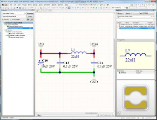
7. Then I create a simple project to which I add the PcbLib and SchLib files I created in the previous steps. The project contains a single Schematic Document with the circuit shown below.

8. I add a new blank PcbDoc to the project which I’ve called InductorExample.PcbDoc. From the PCB editor I run the “Tools->Import Changes From InductorExample.PrjPCB” command to generate an ECO that will add the nets and components to the PCB.
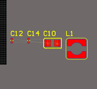
After accepting the ECO changes, the state of the InductorExample.PcbDoc is shown below. The regions that we added to the SRR5028 were treated as an extension to the component pads and consequently the nets that were applied to the pads were also applied to these regions.

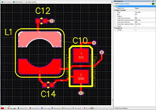
9. I then finish the design by placing the components and adding some routes.
During this editing process, it is important to note that the regions used to define the custom pad shapes continue to be treated by the PCB editor as a separate object.
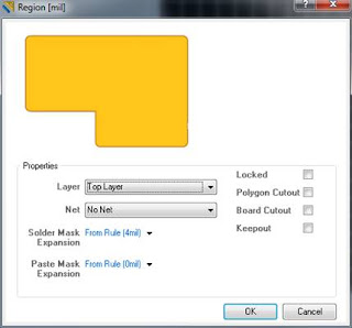
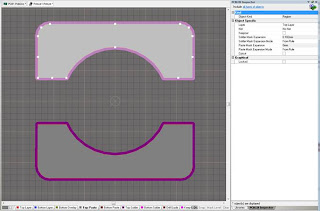
For instance, when the region defining such a custom shaped pad is selected, the inspector shows the properties of a region (and not one of a pad). In this case, it indicates that the Solder Mask expansion of the region in the SRR5028 footprint is 4mil, and is been set by the design rule.

With these enhancements, it should now be much simpler and straightforward to efficiently create and use custom pad shapes.
I’m looking forward to reading your comments and thoughts on the approach we’ve taken, in the comments section below. These have shown to be very insightful and ultimately very useful in helping us provide you with a more streamlined and productive tool.
Thank you very much for your contribution! I am looking forward to reiterate this experience for new projects in the future.

